do you know? The smartphone in your hand integrates the most advanced technology of mankind. It is one of the most cutting-edge achievements of human intelligence. With a smart phone with a high technology content, many people may not believe it?
It seems that money can be made to make mobile phones, but this is mainly due to the relatively developed and sound mobile phone industry chain. In fact, many mobile phone manufacturers are essentially assembly plants and do not have much core technology. Once key components are disabled, they will be Stuck your neck. Because the production of core parts on mobile phones requires high technology, it is not something you can imitate if you want to imitate it.
A smart phone is essentially a mobile computer. The core part is the CPU. It is as important as the human brain, and the performance of a smart phone mainly depends on it.
The first computer in the world was about the size of a small house, and now the computing performance of a fingernail-sized CPU has far surpassed that time. The reason for such a dramatic change is mainly due to the increasing number of integrated transistors per unit area.
Generally speaking, the greater the number of transistors, the stronger the performance of the chip. When some manufacturers advertise the performance of their CPUs, they will advertise how many transistors their CPUs integrate.
The transistors are connected together to form a complex logic circuit. The CPU is a very large-scale integrated circuit that is packaged and has specific functions. Its main ability is to process massive amounts of data.
Now the computer still uses the von Neumann architecture, and the CPU is the most critical part. It mainly contains three parts: a cache memory, a controller, and an arithmetic unit. Take a mobile phone as an example. In addition to the CPU and internal memory, the screen, microphone, speaker, sensor, etc. of the mobile phone are all input and output devices.
If the size of the transistor is reduced, more transistors can be integrated per unit area, so that low power consumption can be achieved while maintaining high performance. Therefore, in addition to the architecture, CPU updates and upgrades often involve efforts in process technology.
The mass production process of the world’s most advanced mobile phone CPU has reached the 5-nanometer level, but the size of the transistor is approaching the physical limit. Because the physical size of silicon atoms is on the order of 0.1 nanometers, no matter how small the size of silicon transistors is, it cannot be smaller than silicon atoms!
At present, a mobile phone CPU can hold more than 10 billion transistors, and it can be calculated that hundreds of millions of transistors are integrated per square millimeter. It is unimaginable to plug so many transistors in such a small space, so some people even think that this technology comes from an alien civilization, but it is really invented by humans.
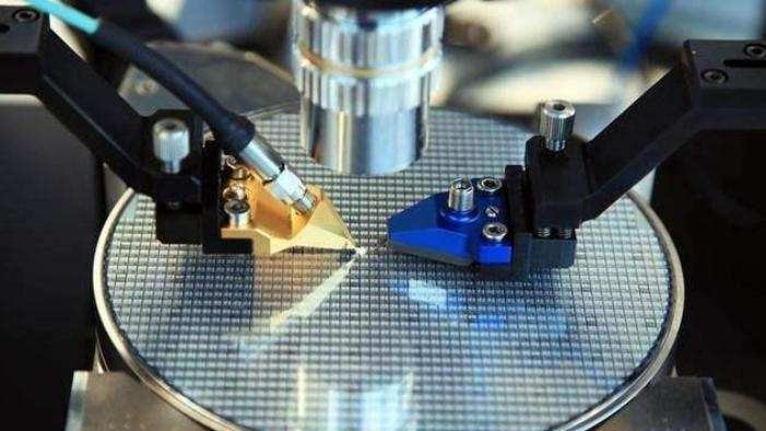
Today’s integrated circuits are generally based on silicon-based semiconductors, so how do so many transistors fit on a small silicon-based wafer?
In fact, such a small chip is not directly manufactured and then assembled into one piece. Instead, it is manufactured directly on the wafer like building blocks, or by lithography. Moreover, with the current human technology level, single manufacturing and then assembling cannot be completed at all.
When it comes to chip manufacturing, everyone will think of lithography machines. To manufacture transistors at the nanometer scale, tools such as tweezers and soldering irons are definitely not acceptable. Light is needed, usually extreme ultraviolet light. The lithography machine is designed specifically to manufacture large-scale integrated circuits based on this, and it mainly acts as a knife. The more advanced the cutter, the higher the etching accuracy, and the smaller the CPU manufacturing process that can be manufactured. At present, this advanced equipment is only mastered by a few companies in the world. In the entire chip production process, the lithography part is also the most complicated and important.
The natural material for making CPUs is actually sand. The main component of sand is silicon dioxide. What we want is almost 100% pure silicon, which is used to make silicon wafers.
The diameter of the wafer is generally 200 mm or 300 mm, and the thickness is 0.5 to 1.5 mm. Wafer manufacturing is the first step in CPU manufacturing, but many are stuck in this step. This is because the purity of silicon and the polishing precision of silicon wafers are very high during the production process.
The logic circuit of the chip is composed of a combination of transistors, usually a MOS tube, and the full Chinese name is called a metal oxide semiconductor field effect transistor. This kind of transistor consists of three parts: gate, source and drain.
After the wafer is manufactured, it is necessary to deposit a layer of silicon dioxide film on its surface by high-temperature heating, and then evenly coat the photoresist, so that it can be used for exposure and etching. The photoresist mainly plays a protective role, and the photoresist after being irradiated by ultraviolet rays can be washed away in the subsequent process.
The circuit diagram of the chip is designed through professional software, and then the photomask is designed accordingly. A chip usually contains many layers of circuits, so many photomasks are needed, and each photomask is very complicated.
The light passes through the photomask, and after being reduced several times by the lens, it will illuminate the wafer, and the photoresist irradiated by the ultraviolet rays will be washed away, so that the circuit diagram is engraved on the wafer. Then the exposed silicon dioxide layer and part of the wafer are etched away to form trenches, and ion implantation is used to dope in specific areas to form PN junctions. Since the transistor is 3D and has 3 poles, it needs to be etched many times to complete the transistor.
And it is too wasteful to make only one layer of circuit on a plane. We usually superimpose many layers, and each layer is isolated by an insulating layer, and between the layers, the transistors and the transistors are connected by metal wires. Metal wires are also manufactured through processes such as etching and deposition. Repeat the above steps many times, and the chip circuit is basically completed.
Finally, the wafer is cut and packaged, and the finished product is tested. As long as the performance meets the requirements, it can basically be packaged and shipped out.
It can be understood from the above that the difficulty of making a mobile phone CPU is indeed greater than that of making an atomic bomb. If it were not for the “Nuclear Non-Proliferation Treaty” restrictions, I believe that many countries in the world could build atomic bombs. Regardless of whether it is to make a CPU or an atomic bomb, the principles are basically disclosed. The difficulty is that the precision required to make a CPU is very high. If any link is not passed, you can get stuck.
In fact, in addition to chip manufacturing, chip design is also a very deep and very important knowledge. If you can’t design a device, let alone manufacturing.